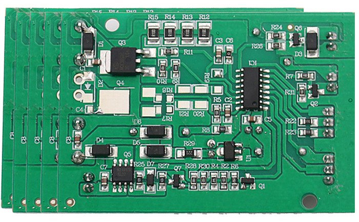
With over five years of expertise in PCB prototyping and fabrication, PCBYES is dedicated to meeting the diverse needs of our clients across various industries. Our commitment to quality, timely delivery, cost-effectiveness, and the ability to handle demanding requirements has made us a trusted name in the PCB industry. Backed by a team of experienced electronics engineers, we offer comprehensive PCBA turnkey services, ensuring the highest customer satisfaction and product quality standards. At PCBYES, we pride ourselves on being more than just a supplier; we aim to be your reliable business partner and a supportive friend in every aspect of your PCB or PCBA needs.
Addressing Surface Blistering Issues in High-Frequency PCBs
Surface blistering in high-frequency PCBs is fundamentally a problem of poor adhesion, which can be traced back to surface quality issues. These issues primarily fall into two categories:
1. Surface Cleanliness: Contaminants or residues on the PCB surface can compromise adhesion.
2. Microscopic Roughness (or Surface Energy): Inadequate surface roughness can hinder proper bonding between layers.
All instances of surface blistering in high-frequency PCBs can be attributed to these root causes. Poor interlayer adhesion fails to withstand the stresses induced during subsequent manufacturing processes, such as mechanical, thermal, or plating stresses, leading to layer separation and blistering.
Key Factors Contributing to Surface Quality Issues in High-Frequency PCBs
1. Substrate Processing Issues:
Thin substrates (typically less than 0.8mm) pose a challenge due to their low rigidity, making them unsuitable for mechanical brushing. Inadequate removal of the protective oxide layer during processing can result in poor adhesion between the copper foil and chemical copper, leading to blistering. Similar issues can arise during black oxide or browning processes, where uneven coloration or incomplete treatment may occur.
2. Contamination During Mechanical Processing:
Drilling, lamination, and edge milling can introduce oils, dust, or other contaminants, compromising surface quality and adhesion.
3. Poor Brushing Before Electroless Copper Deposition:
Excessive brushing pressure can deform via openings, expose substrate material, or increase copper roughness, leading to blistering during subsequent processes like plating or soldering. Proper brushing parameters must be optimized through scratch and water-break tests.
4. Inadequate Rinsing:
Insufficient rinsing after chemical treatments can leave residues, causing localized adhesion issues. Factors such as water quality, flow rate, rinsing time, and drip time must be carefully controlled, especially in colder temperatures where rinsing efficiency decreases.
5. Micro-Etching in Pre-Treatment Processes:
Over-etching can expose substrate material while under-etching can result in poor adhesion. Optimal micro-etching depths are 1.5–2 µm for electroless copper and 0.3–1 µm for pattern plating. Visual inspection of the surface (uniform pink color, no gloss) and monitoring of copper content, temperature, and etchant concentration are critical.
6. Issues with Electroless Copper Rework:
Improper stripping methods or excessive micro-etching during rework can cause blistering. For panels with thickened copper, controlled stripping followed by light brushing and adjusted micro-etching is recommended.
7. Oxidation During Production:
Exposure to air or prolonged storage in acidic solutions can oxidize copper surfaces, leading to blistering. Electroless copper panels should be processed within 12 hours to prevent oxidation.
8. Overly Active Electroless Copper Solution:
High copper content or excessive activity in the electroless copper bath can result in rough deposits, hydrogen entrapment, or poor adhesion. Adjustments such as diluting the solution, increasing complexing agents, or lowering bath temperature can mitigate these issues.
9. Contamination During Pattern Transfer:
Inadequate rinsing after development, prolonged exposure to dust, or poor handling can compromise surface cleanliness and adhesion.
10. Organic Contamination in Plating Baths:
Oil or organic contaminants in plating baths, particularly in automated lines, can lead to surface defects.
11. Acid Dip Tank Contamination:
High copper content or contaminants in the acid dip tank can affect surface cleanliness and roughness.
12. Temperature Control in Winter:
In colder temperatures, preheating rinse tanks (30–40°C) before nickel plating can ensure dense and uniform nickel deposition.
Surface blistering in high-frequency PCBs is a multifaceted issue influenced by various factors, including substrate processing, contamination, chemical treatments, and environmental conditions. At PCBYES, we leverage our extensive experience and advanced techniques to address these challenges, ensuring the highest quality standards for our clients. Whether you require high-frequency PCBs, PCBA turnkey services, or expert guidance, PCBYES is here to support your every need.


